Almost all electronic devices have PCB boards, from household electronic watches, calculators, communication electronic equipment, to military weapon systems. This also means that as long as there are electronic components such as integrated circuits, in order to interconnect them, we must use printed circuit boards. Let’s follow the turnkey PCB assembly company FS Technology to see the classification and process flow of pcb equipment.
PCB production process

In the study of large electronic products, the most fundamental success factor is the design, manufacture and assembly of printed circuit boards. PCB design and manufacturing directly affect the quality and cost of the product. This determines whether a business can succeed when competing.
PCB manufacturing process: incoming plate→pickling→pump washing→city washing→four brushes with swing plate→high pressure infusion pump washing (20 Kg/cm 2 )→pump cleaning→city washing→suction→drying→drying→discharging.
In electronic devices, PCBs provide the following functions:
- Provide mechanical support for the fixing and assembly of electronic components such as integrated circuits.
- Realize wiring and electrical connection or electrical insulation between various electronic components such as integrated circuits.
- Provide the required electrical characteristics, such as characteristic impedance, etc.
- Solder mask graphics for automated soldering, identifying characters and graphics for component insertion, inspection and maintenance are provided.
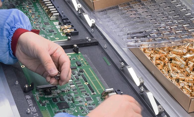
For some companies that do not have their own factories, assembling printed circuit boards is very troublesome. You can take a look at the FS Technology PCB component capabilities. We can meet the needs of most customers.
Basic terms related to PCB
On the insulating substrate, according to a predetermined design, a printed circuit, a printed element or a combination of two conductive patterns is made, which is called a printed circuit.
Because the PCB can provide electrical connection channels for the components, the conductive pattern of the device is called a printed circuit. Electronic components are assembled by a one-stop PCB assembly company.
The printed circuit board is called a PCB board, also called a PC board, and the assembled PCB board is called a PCBA board.
Classification of PCB boards
According to the degree of rigidity and flexibility of the substrate: rigid printed circuit board board, flexible PCB board and rigid-flex PCB board.
According to the number of layers of the PCB: single-sided, double-sided and multi-layer printed boards.
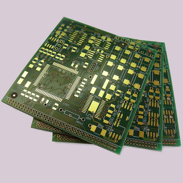
The position of conductor pattern and substrate: flat printed board and curved printed circuit board.
The use of printed boards in electronic equipment avoids errors in manual wiring due to the printed board-like consistency. Through a turnkey PCB assembly company, we can help you realize automatic insertion or installation of electronic components, automatic welding and automatic detection, which ensures the quality of electronic equipment, improves labor productivity, reduces costs, and facilitates maintenance.
Printed circuit boards (PCBs) have developed from single-layer to double-sided, multi-layer and flexible, and have maintained their respective development trends. Due to the continuous development in the direction of high precision, high density and high reliability, and the continuous reduction of size, cost and performance, printed circuit boards will still maintain strong vitality in future electronic equipment development projects.
A sign of the level of PCB technology
The skill level of a turnkey PCB assembly company depends on the fabrication of double-sided and porous metallized printed boards. The manufacture of porous metallized printed boards is the standard of qualification for turnkey companies. FS Tech can achieve high volume production of double-sided metal printed boards. We can also record the number of conductors for you if you need it.
FS Technologies will place wires between the two pads if using low density PCBs with trace widths greater than 0.3 mm. Place two lines between the two pads of the MDF with a line width of about 0.2 mm. If FS Technology uses a high density board with a line width of about 0.1 – 0.15mm, it will place three lines between the two pads. To sum up, we can see that the density of the board depends on the number of lines between the pads. For example: when we use an ultra-high density printed circuit board with a line width of 0.05-0.08mm, four lines need to be laid between the two pads.
PCB production and assembly equipment
PCB production and assembly equipment includes deburring machine, double-sided alkaline etching machine, metal chemical cleaning machine, etching production line…
FS Technology will use a deburring machine to remove burrs and surface oxide layers from printed circuit boards. 30Kg/cm 2 high pressure cleaning pump, can thoroughly remove burrs and surface dirt.

1. PCB system equipment.
printed circuit board electronic film developing and fixing automatic processor.
Machine nozzles for developing, plating, etching and film removal.
2. PCB machining equipment.
Including vacuum laminating machine, PCB substrate grinding machine, PCBs forming machine, PCB inner layer fusing machine, automatic centering fusing machine and PCBs punching machine.
3. Electroplating/wet process equipment.
From the development of etching to the electroless nickel plating to the gold production line and finally to the PCB production line.
4. Screen printing/dry process equipment.
Provide various UV curing machine – precision hot air oven, oven – man-machine interface UV – CM – 650 type plate cleaning machine.
FZ J – 60J / FZJ – 80J / F – ZZ – 90J Vertical Flat Screen Printing Machine.
5. printed circuit board testing/quality control equipment.
C MI 900X Fluorescent Coating Thickness Gauge – C CI 563 Surface Copper Thickness Tester
HOLINK precision (ventilated) high temperature testing machine—HO LINK large-scale constant temperature and humidity laboratory.
WALCHEM Automatic Nickel Plating Controller
COMPACT ECO – printed circuit boardType X-Ray Fluorescence Coating Thickness Gauge – Test Fixture Test Bench
SWET – 2100e Solderability Tester – Gold Dot Electronic High Voltage Tester
6. SMT welding installation equipment.
The stainless steel semi-automatic slag reduction machine, automatic spray welding and wave soldering are changed to lead-free operation.
7. other electronic equipment.
In addition to the use of PCBs ink mixing equipment and bidirectional rotary ink mixing machines, Chinese printed circuit board manufacturers also use circuit board drilling wooden pads and aluminum, PCB ink mixing machines and tin dross reducers.